PCB marking machines today cut down on prototype waste somewhere between 18 to 34 percent when compared with old fashioned manual techniques thanks to their incredible alignment accuracy below 25 micrometers. When components get labeled wrong or drilling goes off track, whole boards end up getting tossed out, but these machines prevent exactly that kind of problem. The vision guided systems actually have real time optical corrections built in so they can keep registration within plus or minus 0.01 mm. That level of precision is really important when dealing with those densely packed circuit connections. Getting layout issues sorted out at the beginning saves everyone from having to do massive amounts of rework later on. According to some recent research from the Electronics Prototyping Trends Report last year, this early detection approach alone handles around two thirds of all material waste during prototyping phases.
Leading manufacturers align DFM checks with PCB marking machine capabilities during CAD drafting. This integration identifies issues such as:
Resolving these constraints before fabrication reduces post-production corrections by 41% while preserving design integrity.
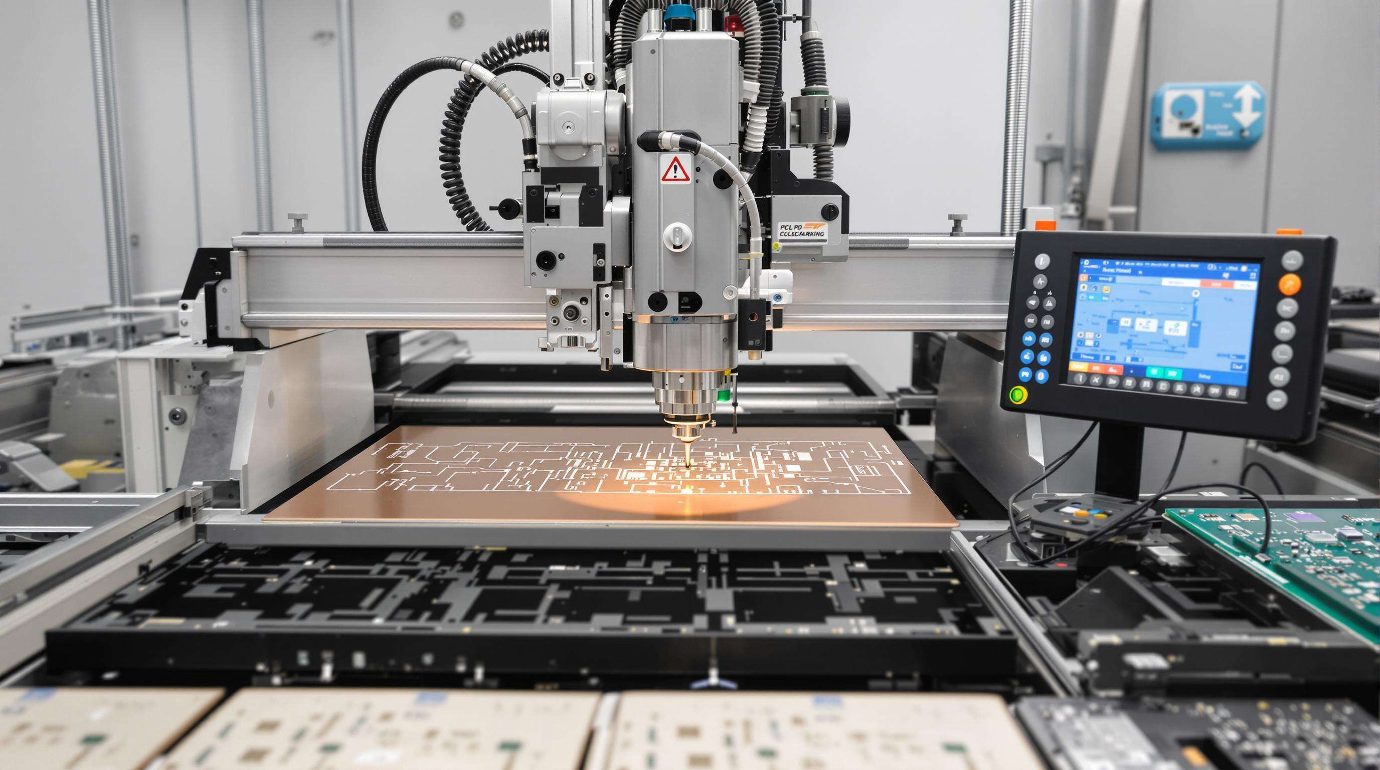
Combining 6-axis CNC milling with UV laser marking achieves under 0.05mm feature accuracy across substrates like FR4 and flexible polyimide. The integrated workflow enhances precision and reduces waste at every stage:
| Step | CNC Action | Marking Machine Role | Waste Impact |
|---|---|---|---|
| 1 | Route board outline | Engrave fiducial marks | -22% panel scrap |
| 2 | Drill microvias | Label polarity indicators | -15% assembly errors |
| 3 | Surface finishing | Apply solder mask annotations | -30% reflow defects |
This closed-loop process delivers first-article success rates above 89%, significantly outperforming decoupled systems at 62%.
The chemical etching process creates roughly three times as much hazardous waste as CNC milling does because it uses stuff like ferric chloride, which costs a lot to get rid of properly so we don't mess up the environment. Dry milling on the other hand leaves behind nothing but non toxic copper dust that can be recycled or thrown away without worries. According to research published last year in a sustainability report for manufacturers, switching from etching to milling cuts down on wasted materials during prototyping by around 40 percent. This difference becomes even bigger when companies align their PCB marking machines correctly, making sure they use every inch of the boards before cutting anything else.
The precision of PCB milling gets a major boost when marking machines handle those sub 4 micrometer fiducial alignments right before the CNC work starts. What this means for manufacturers is far fewer headaches down the line since the toolpaths end up exactly where they need to be. The real money saver comes from cutting out around 12 to 15 percent waste that usually happens during manual alignment steps in traditional etching methods. And there's another perk too – many modern systems now include integrated laser marking features that check those critical trace widths as they go along. When something looks off, operators can jump in and fix it right away before problems like multilayer board separation or connectors sitting at odd angles become expensive issues later on.
One hardware startup managed to cut down on prototype waste by nearly two thirds when they combined a four axis CNC mill with a dual laser PCB marker. The automated design for manufacturing checks caught those tricky via placements that couldn't be made before actual milling started happening. Plus those UV markings became really handy as permanent reference points during assembly. The results were pretty impressive too copper clad laminate consumption went way down from 22 sheets each month to just 8. This dramatic reduction helped them get their ISO 14001 environmental certification in under half a year, which was quite an accomplishment for such a small shop.
Regular recalibration using ISO-certified tools maintains ±0.005mm positional accuracy in PCB marking machines, preventing misaligned drill holes and traces. Thermal compensation protocols counteract machine expansion during prolonged runs—particularly important when processing thermally sensitive materials like polyimide.
Advanced CAM software analyzes copper thickness and tool wear to generate optimized milling paths, reducing unnecessary bit retractions by 18%. Adaptive clearing strategies minimize substrate stress, and when combined with data from the PCB marking machine, cut material waste by 22% compared to conventional workflows.
Modern systems enable real-time design rule checks (DRC) between CAD software and PCB marking machines, eliminating 96% of dimension-related scrap errors. Bi-directional data exchange reduces manual file adjustments by 65%, especially beneficial for complex HDI layouts with micro-vias under 0.15mm.
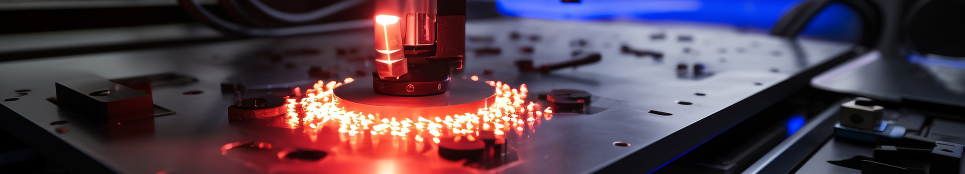
Modern PCB marking machines now come equipped with optical sensors combined with machine learning algorithms that can spot tiny deviations at the micron level during the prototyping stage. When these systems catch something off track, they provide immediate feedback so bad batches don't move forward through the process. According to research published by Ponemon in 2023, this approach cuts down on wasted materials by around 34% compared to what happens with just regular manual checks. The technology doesn't stop there either. These smart systems will actually tweak their settings on their own or even bring production grinding to a halt whenever measurements go beyond acceptable limits. What does all this mean? Consistently good quality products without needing constant oversight from humans throughout the manufacturing line.
Uniform marking parameters—such as speed, pressure, and depth—reduce alignment errors by 27% across prototyping phases (IPC 2024). Centralized protocols ensure compatibility between marking systems and downstream processes like soldering or coating. For instance, standardized fiducial markers improve robotic assembly accuracy by 19%, reducing rework from misalignment.
According to an industrial report from 2025, around two thirds of new electronic companies are focusing on automating their printed circuit board marking processes these days. These businesses see their waste levels drop by about 40 percent compared to what's normal across the sector. The move towards automation actually helps meet those ISO 14001 standards many companies strive for. When manufacturers connect their marking equipment to the cloud, they get detailed records that show exactly how green their operations really are. For startups employing artificial intelligence in their marking systems, the results speak volumes. They manage to get products right on the first try about 92 times out of 100, which means far fewer rounds of testing and redesigning. Future Market Insights backs this up with their research findings.
PCB marking machines significantly enhance precision and reduce waste. They achieve alignment accuracy below 25 micrometers, minimizing errors and the need for rework, thereby saving material waste.
Leading manufacturers align DFM checks with PCB marking machine capabilities to identify design constraints early, reducing post-production corrections by 41% and maintaining design integrity.
Yes, chemical etching creates roughly three times as much hazardous waste compared to CNC milling, which primarily leaves non-toxic copper dust. Transitioning to milling can cut wasted materials by up to 40%.
Modern PCB marking machines equipped with optical sensors and machine learning algorithms can detect micron-level deviations, providing real-time feedback to prevent issues from progressing through manufacturing.


